


 cn
cn
Home
> News > From PCBA manufacturing to one-stop solutions: Hanpu Intelligent Manufacturing leverages PCBA manufacturing as a fulcrum to drive end-to-end hardware
From PCBA manufacturing to one-stop solutions: Hanpu Intelligent Manufacturing leverages PCBA manufacturing as a fulcrum to drive end-to-end hardware
 2026.07.09
 406
406Hanputek's One-Stop PCBA Service Analysis: Empowering AI Computing, Robotics, and Smart Hardware from Design to Mass Production
In 2026, as the global electronics manufacturing industry undergoes profound transformation, the explosive growth of artificial intelligence (AI) technology is reshaping the entire industrial chain landscape. As a core link in electronics manufacturing, PCBA (Printed Circuit Board Assembly) carries the critical mission of transforming design blueprints into highly reliable, functional hardware. Facing the surge in demand driven by AI servers, high-performance computing, intelligent robotics, and edge devices, Hanputek—a one-stop PCBA smart manufacturing service provider from China's Pearl River Delta—is leveraging its full-chain service system covering design, manufacturing, quality control, and supply chain to become a key driving force behind AI hardware innovation, from proof-of-concept to large-scale mass production.
Structural Growth in the Global PCBA Market, with AI Hardware as the Core Engine
According to a report by market research firm Grand View Research, the global PCBA market is projected to grow from approximately \$98.9 billion in 2025 to \$137.4 billion by 2033, at a compound annual growth rate (CAGR) of 4.3%. Meanwhile, data jointly released by Taiwan's TPCA (Taiwan Printed Circuit Association) and ITRI (Industrial Technology Research Institute) indicates that, driven by demand for AI servers and high-performance computing, global PCB output value is expected to reach \$105.2 billion in 2026, representing a year-on-year increase of 13.9%.
This wave of growth is not a simple expansion in scale, but rather a profound structural upgrade in demand. AI computing hardware places demands on PCBA that far exceed those of traditional consumer electronics: higher layer counts (32-layer and above high-order HDI boards), more stringent signal integrity requirements, more complex thermal management, and near-zero-defect reliability standards. At the same time, as demand for traditional consumer electronics slows, AI servers, data center accelerator cards, intelligent robots, and edge computing devices are becoming the strategic high ground that PCBA manufacturers are competing for.
It is against this backdrop of industry transformation that Hanputek has positioned itself as "a PCBA one-stop service provider focused on AI applications," deeply engaging with the hardware realization needs of AI computing enterprises, robotics manufacturers, and smart hardware innovators.
Design Empowerment: AI-Assisted Simulation and Signal Integrity Analysis to Reduce Trial-and-Error Costs from the Source
PCBA design marks the starting point of a product's lifecycle and is the most critical stage determining cost, performance, and manufacturability. Traditional design processes rely heavily on individual engineers' experience and repeated trial and error. For highly complex projects such as AI accelerator cards and high-performance computing motherboards, this often requires iteration cycles spanning weeks or even months, and manufacturability defects are prone to surface later in the manufacturing stage.
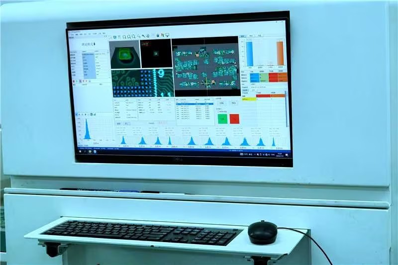
According to Hanputek's internal statistics, this design front-loading capability has significantly reduced the number of prototype iterations required by clients, with the first-pass yield rate for engineering samples notably exceeding the industry average. This not only substantially reduces material waste and time costs during the R&D phase, but also lays a solid foundation for yield improvement during subsequent mass production.
Manufacturing Synergy: AI-Driven Smart Scheduling and Precision Mounting, Balancing Rapid Prototyping with Scaled Production
Moving into the SMT (Surface Mount Technology) and assembly stages, Hanputek leverages the well-developed electronics industry ecosystem of the Pearl River Delta to build a flexible manufacturing network covering everything from rapid prototyping and small-to-medium batch trial production to mass production at the scale of tens of millions of units. Its core advantage lies in the deep integration of AI-powered intelligent scheduling systems with high-precision mounting processes.
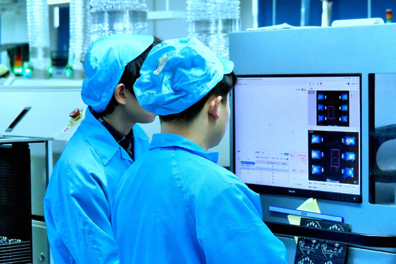
At the process execution level, Hanputek employs AI-enhanced machine vision and position calibration technology to ensure precision mounting of highly complex components such as 01005 micro-components, 0.3mm-pitch BGAs, and POP (Package-on-Package) stacked packages, precisely meeting the advanced packaging process requirements of AI processors and high-bandwidth memory chips. Meanwhile, predictive maintenance systems continuously monitor the operating status of key equipment such as reflow ovens and pick-and-place machines, effectively reducing the risk of unplanned downtime and ensuring the continuous, stable delivery of large-scale orders.
Intelligent Quality Control: AI Deep Learning Inspection Builds a Zero-Defect Delivery Defense Line
The stringent reliability requirements of AI hardware make quality control one of the most heavily weighted aspects of PCBA services. A microscopic void in a single BGA solder ball or a micron-level scratch on a circuit trace can cause a catastrophic failure in an entire AI server or intelligent robot during operation.
Hanputek embeds quality control throughout the entire production process, building a multi-layered intelligent inspection system covering fully automated AOI (Automated Optical Inspection), X-Ray inspection, SPI (Solder Paste Inspection), and ICT (In-Circuit Testing). Unlike traditional AOI systems that rely on fixed algorithms and are prone to missing concealed defects, the AI deep learning inspection models deployed by Hanputek continuously learn the morphological characteristics of various defect types, achieving precise identification of micron-level defects such as BGA solder joint voids, cracks, misalignment, and foreign particles.
Actual production data shows that this AI-enhanced quality control system maintains a defect detection rate consistently above 98%, while false alarm rates are reduced by more than half compared to traditional equipment. Combined with SPC (Statistical Process Control) and closed-loop process feedback mechanisms, production lines can adjust printing parameters and reflow soldering temperature profiles in real time, forming a rapid "detect—analyze—adjust" closed loop. This capability allows Hanputek to consistently maintain near-zero-defect manufacturing (ZDM) standards in the delivery of high-reliability products such as AI servers and intelligent robots.
Supply Chain Resilience: AI Forecasting and a Global Procurement Network to Address Material Delivery Volatility
The high-end substrates, high-speed connectors, and high-performance computing chips required for AI hardware have long faced risks of tight supply and price volatility. Geopolitical conflicts and tariff policy adjustments further exacerbate supply chain uncertainty.
Hanputek relies on an experienced supply chain team and an AI-driven market analysis system to monitor global component price trends, lead time changes, and the availability of alternative components in real time, providing clients with flexible stocking strategies and early warnings. Through intelligent demand forecasting and dynamic inventory management, Hanputek helps clients reduce the risk of critical material shortages by one-third, significantly shortening overall project delivery cycles. At the same time, a multi-source procurement strategy and regionalized production capacity deployment effectively strengthen resilience against international trade friction, safeguarding supply chain continuity for global clients.
Service Model Innovation: A One-Stop Closed-Loop System Accelerating AI Hardware Productization
The essence of Hanputek's one-stop PCBA service is not a simple stacking of capabilities across different stages, but rather a closed-loop service system centered on manufacturing, extending forward into design consulting and DFM review, and backward into full system assembly and testing delivery.
For AI startups and clients transitioning from other industries, Hanputek offers a "Productization Acceleration Program"—covering hardware architecture assessment, key component selection, prototype trial production, and mass production ramp-up, with a dedicated project manager and technical support team providing end-to-end coordination. This model effectively addresses common pain points faced by AI hardware innovators in the "design—manufacturing—delivery" chain, such as communication gaps, poor process adaptation, and inconsistent quality standards, helping clients complete the leap from R&D concept to scaled product with lower risk and shorter cycles.
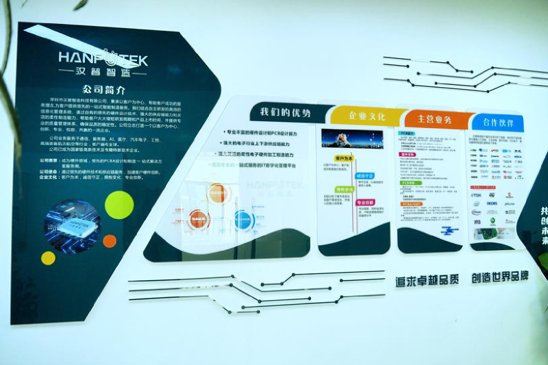
From a broader perspective, PCBA manufacturing is one of the cornerstones of the global competitiveness of China's electronics information industry, and an important vehicle for "new quality productive forces" in advanced manufacturing. Hanputek's focused investment in the AI direction aligns closely with the broader trajectory of China's manufacturing industry toward high-end, intelligent, and green development.
As generative AI continues to penetrate edge devices and new materials and processes such as glass substrates and advanced packaging gradually reach commercialization, the PCBA industry is entering a new technology cycle. Hanputek states that it will continue to increase R&D investment in AI design automation, intelligent inspection algorithms, and digital twin manufacturing, driving its service model to evolve continuously from "professional manufacturing" toward "data-driven intelligent manufacturing services."

Contact information


Services
Industries
News
About Us